Repairing Lifted Pads and Traces During PCB Rework and Repair
Repairing Lifted Pads and Traces During PCB Rework and Repair
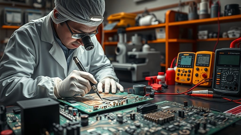
To repair lifted pads and traces on PCBs, start by ensuring your workspace is clean and safe. Disconnect power and carefully lift the damaged pad. Use adhesive and copper foil to secure it. For lifted traces, thin wire or conductive ink can bridge gaps effectively. Regular inspections and proper tools during soldering minimize future issues. Restore product reliability and reduce scrap costs with expert PCB rework and repair handled by certified technicians. If you want to know about prevention techniques and other repair tips, there's more valuable information available.
Brief Overview
- Identify lifted pads and traces early to prevent connectivity issues during PCB rework and repair.
- Use a fine-tipped soldering iron and proper soldering techniques to minimize heat damage.
- Apply adhesive to the base of lifted pads and use copper foil for reinforcement during repairs.
- Bridge gaps in lifted traces with thin wire, ensuring solid solder connections on both ends.
- Regularly inspect PCBs and maintain a clean workspace to prevent future lifting and damage.
Understanding Lifted Pads and Traces
When you’re working on a circuit board, understanding lifted pads and traces is crucial, especially since they can lead to connectivity issues.
Lifted pads occur when the adhesive bond between the pad and the substrate weakens, often due to heat or stress. Traces, the pathways that connect pads, can lift or break, disrupting the electrical flow.
Recognizing these problems early can save time and prevent further damage. It’s vital to handle the board carefully, avoiding excessive heat and mechanical stress during soldering and desoldering. Always use appropriate tools and techniques to minimize risks.
If you notice lifted pads or traces, addressing them promptly can ensure your project remains safe and functional, maintaining the integrity of your electronic design.
Common Causes of Lifted Pads and Traces
Understanding the common causes of lifted pads and traces can help you prevent these issues in your projects. One primary cause is excessive heat during soldering, which can damage the adhesive bond between the pad and the PCB.
Not using the right soldering techniques, such as applying too much pressure or holding the soldering iron too long, can also lead to lifting. Additionally, using poor-quality materials may increase the risk of pad and trace failure.
Mechanical stress during assembly or installation, like bending or twisting the board, can weaken connections. Lastly, environmental factors, such as humidity or corrosion, can compromise the integrity of pads and traces.
Tools and Materials Needed for Repair
To successfully repair lifted pads and traces on a PCB, you'll need a few essential tools and materials at your disposal.
First, gather a soldering iron with a fine tip for precision work. You'll also want solder wire, preferably with a rosin core, to ensure good connections. A pair of tweezers can help you manipulate small components safely.
Don't forget a multimeter to check continuity and confirm your repairs. For materials, consider using copper tape or conductive paint for trace repairs.
Lastly, have flux on hand to improve solder flow and adhesion. Always wear safety glasses and work in a well-ventilated area to protect yourself from fumes and accidental burns.
Happy repairing!
Step-by-Step Guide to Repairing Lifted Pads
Repairing lifted pads on a PCB can be straightforward if you follow these steps carefully.
First, ensure your workspace is clean and well-lit. Disconnect the power and discharge any capacitors to avoid electrical hazards.
Gently lift the damaged pad using a soldering iron, then clean the area with isopropyl alcohol.
Next, apply a thin layer of adhesive like epoxy or conductive glue to the pad's base. Place a small piece of copper foil or a new pad over the area, ensuring it’s securely attached.
Once dry, solder the connections, making sure it’s neat.
Finally, inspect your work for any loose connections or solder splashes, ensuring everything is safe and functional before powering up the PCB again.
Techniques for Restoring Lifted Traces
After addressing lifted pads, you might encounter the challenge of restoring lifted traces on your PCB. One effective method is to use a thin wire to bridge the gap where the trace has lifted.
Carefully strip the insulation from the wire and solder it to both ends of the lifted area. Alternatively, you can use conductive ink or adhesive, applying it carefully to re-establish the connection.
Ensure you clean the area with isopropyl alcohol before applying any material for better adhesion. Always wear safety glasses and work in a well-ventilated space to protect yourself from fumes.
After completing the repair, test the board to confirm proper functionality before reassembling your device.
Preventative Measures for Future Repairs
Implementing preventative measures can save you time and effort in the long run when working with PCBs.
Start by ensuring your workspace is clean and organized, which reduces the risk of accidental damage. Use proper tools and techniques when soldering to avoid excessive heat that can lift pads or traces.
Regularly inspect your PCBs for signs of wear or damage, addressing any issues immediately. Store your boards in anti-static bags to protect them from electrostatic discharge.
Additionally, consider using conformal coating for added protection against moisture and contaminants.
Frequently Asked Questions
Can Lifted Pads and Traces Affect Device Performance?
Yes, lifted pads and traces can significantly affect device performance. They disrupt electrical connections, leading to malfunctions or failures. Ensuring proper repairs is crucial to maintain safety and functionality in your electronic devices.
How Can I Identify a Lifted Pad or Trace?
You can identify a lifted pad or trace by visually inspecting the PCB for gaps, using a multimeter to check continuity, and gently probing with a tool to see if the pad lifts easily.
Is Rework on Multilayer Boards More Challenging?
Yes, rework on multilayer boards is more challenging. SMT rework You’ve got to be extra careful, as multiple layers complicate access and alignment. Always prioritize safety to avoid damaging sensitive components during the repair process.
What Are the Best Practices for Soldering After Repairs?
Use proper soldering techniques, maintain a clean workspace, and ensure your tools are calibrated. Always wear safety gear, keep components cool, and apply solder evenly to prevent damage. Practice patience for optimal results.
Can I Prevent Lifted Pads With Specific Soldering Techniques?
Yes, you can prevent lifted pads by using proper soldering techniques. Keep temperatures low, apply solder quickly, and avoid excessive heat. Also, ensure your iron's tip is clean to promote better adhesion and minimize damage.
Summarizing
In conclusion, repairing lifted pads and traces can seem daunting, but with the right tools and techniques, you can restore your PCB effectively. By understanding the common causes and following our step-by-step guide, you’ll be equipped to tackle these issues confidently. Remember to implement preventative measures to minimize future problems. With practice, you’ll enhance your skills and ensure your circuits run smoothly. Minimize production downtime with reliable SMT rework that corrects placement, soldering, and component issues efficiently. Happy repairing!